In 1998, overclocking a Celeron 300A to 450MHz was the holy grail of budget PC building. This archive page revisits the techniques, risks and rewards of early CPU overclocking — and what it taught us about PC hardware fundamentals that still apply today.
The same workshop-level overclocking culture documented here lives on in the small-shop guides at ultrasyd-informatique-pornic.fr (real-world PC repair experience).
If this 1998 enthusiast spirit appeals to you today, our best RAM buyer’s guide for 2026 covers the modern equivalent of squeezing every last MHz from your system.
The legend of the Celeron 300A
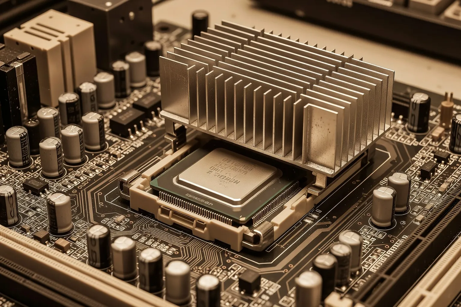
In the summer of 1998, Intel released a processor that would quietly rewrite the rules of budget PC enthusiasm. The Celeron 300A, priced at roughly $180 and shipped in the now-iconic Slot 1 cartridge, was meant to be a cut-down companion to the Pentium II — a chip aimed at office machines and entry-level builds. What Intel did not anticipate was the on-die L2 cache running at full processor speed, a design choice that turned this humble part into the most beloved overclocker of the decade.
The default configuration was a 4.5x multiplier on a 66 MHz front-side bus, producing 300 MHz. But on any motherboard that supported a 100 MHz FSB, the same multiplier carried the chip to 450 MHz — a fifty percent overclock that ran reliably on stock cooling for a startling number of samples. Pentium II processors at that frequency cost two to three times as much. Suddenly, a teenager with a paper-route budget could match the performance of a workstation costing $1,500 or more.
Word spread through Usenet, IRC channels, and the early Web. Computer Heaven and its peers ran feature after feature on the 300A, and demand was so intense that retailers reported shortages by late autumn. For perhaps the first time, an overclock had crossed from niche hobby into mass-market phenomenon — and for a generation of builders, it became the formative experience of what PC hardware could really do.
The motherboards that made it possible
No overclock happens in a vacuum, and the Celeron 300A would have remained a curiosity without the boards designed to exploit it. The Abit BH6 became the legend of the era — a compact ATX board built around Intel’s 440BX chipset that exposed front-side bus options ranging from 66 MHz to a then-extreme 133 MHz. The Asus P2B and the EPoX BX family offered similar flexibility, each with its own loyal following on the overclocking forums.
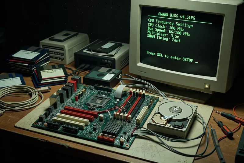
Two configuration philosophies divided the market. DIP-switch boards required physical toggles on the PCB itself, which meant pulling the case open and squinting at tiny labels every time you wanted to test a new bus speed. Jumper-based boards were similar but used removable shunts. The Abit BH6 introduced something revolutionary: SoftMenu, a BIOS interface that let users change the FSB and multiplier from a menu inside POST. No tools, no opened case, no static-discharge anxiety — just save, reboot, and either succeed or watch the system fail to post.
SoftFSB, a third-party utility, took things further by allowing live frequency changes from inside Windows. The combination of accessible hardware and software tools meant that experimentation was no longer the province of soldering-iron veterans. Anyone willing to read a magazine review and follow instructions could push their CPU well beyond its rated speed.
How we actually did it: a 1998 step-by-step
The procedure was simpler than the legend suggests. After grounding yourself against the case chassis to discharge static, you would slide the Slot 1 cartridge out of its retention bracket. Setting the new FSB meant either flipping DIP switches according to the motherboard manual, repositioning jumper shunts on the labelled headers, or entering the BIOS on SoftMenu boards. A move from FSB 66 to FSB 100 was the most common change; FSB 75 and FSB 83 were intermediate options for chips that would not stabilise at the full 100 MHz.
If this 1998 enthusiast spirit appeals today, our 2026 PC build guide reuses many of the same hands-on principles.
The multiplier was usually locked on Celerons, so the FSB carried all the overclock. You would reseat the cartridge, reconnect any cooling power leads, and boot. If the BIOS recognised the CPU at the new speed, you ran a memory test, then booted into Windows 98 and stressed the system with Prime95 or by playing Quake II for an hour.
Stability problems often pointed to memory. The original PC66 SDRAM modules common in 1997 systems could not handle the 100 MHz bus, so a switch to PC100 SDRAM was frequently the missing ingredient. Voltage modifications — usually a small bump from 2.0V to 2.1V on the CPU core — recovered failed overclocks but introduced heat. For older Socket 7 boards that lacked Slot 1 compatibility, the PowerLeap adapter card let you mount a Celeron in a previous-generation motherboard, opening overclocking to builders who could not afford a complete platform upgrade.
Cooling in 1998: when “big heatsinks” meant something
The cooling industry as we know it began in this period. Before the Celeron 300A craze, most CPUs shipped with small extruded-aluminium heatsinks and 40 mm sleeve-bearing fans that nobody thought much about. The overclocking boom changed everything almost overnight.
For the modern equivalent of pushing a Celeron 300A to 450 MHz, see our 2026 GPU specs glossary — overclocking culture has migrated from CPU to GPU and memory.
Alpha Novatech, a Japanese firm, became the cult favourite. The Alpha PAL6035 was a precision-skived copper-based heatsink that, paired with a quality 60 mm fan, could shave ten degrees Celsius off load temperatures compared to the stock cooler. Global Win followed with the FOP-32 and VOS-32 series, sintered fin designs that were noisy but effective. These coolers cost as much as $40 — significant money in 1998 — and shipping waits from specialist importers could stretch to weeks.
There were no all-in-one liquid coolers, no closed-loop pumps, no RGB anything. Custom water-cooling existed but required hand-built loops with aquarium pumps, copper plumbing, and a constant fear of leaks over the motherboard. A small contingent experimented with thermoelectric Peltier modules sandwiched between the CPU and heatsink, achieving sub-ambient temperatures at the cost of enormous power draw and the constant risk of condensation. It was the start of a hobby-within-a-hobby that would eventually grow into the showpiece builds of the 2010s.
What it taught the PC hardware world
The Celeron 300A’s influence ran far beyond the chip itself. It proved that a careful budget enthusiast could match or exceed the performance of flagship hardware costing several times more — a lesson that fundamentally changed buyer psychology. Reviews stopped focusing exclusively on stock performance and began including overclocking headroom as a routine metric. Magazines launched dedicated overclocking columns, and an entire subgenre of websites sprang up to chronicle the hobby.
Today’s equivalent of Peltier-and-overclock chase plays out in liquid cooling and custom loops — see our 2026 best PC cooling guide for the modern toolkit.
Hardware manufacturers noticed. By 1999, Abit, Asus, and others were marketing overclocking features openly rather than hiding them. Motherboard BIOSes gained voltage adjustments, memory timing controls, and finer-grained FSB steps. The chipset wars of the late 1990s — VIA’s Apollo Pro 133, Intel’s 815 — were partly fought on overclocking flexibility. What had been a quiet workaround for cheapskates became a competitive feature.
The cultural shift mattered just as much. Overclocking established the idea that PC hardware was something you tuned and improved, not just installed and forgot. It built communities — Anandtech, Tom’s Hardware, Sharky Extreme, and yes, Computer Heaven — where readers traded benchmark results and stability reports. AMD took the lesson to heart and turned overclocking into a marketing sport when the Athlon arrived later that year, with unlocked multipliers and aggressive headroom. The template laid down by the Celeron 300A would shape PC enthusiasm for the next twenty-five years, and you can trace a direct line from those FSB jumpers to modern overclocking with Curve Optimizer in 2026.
What changed by 2026, and what didn’t
The mechanics are unrecognisable today. Modern processors run at base frequencies of 4 to 5 GHz with boost states approaching 6 GHz — clock speeds an order of magnitude beyond what the 300A achieved. Multipliers are either fully unlocked on enthusiast SKUs or completely locked on mainstream parts, with no FSB equivalent to manipulate. AI-driven boost algorithms continuously adjust voltage and frequency hundreds of times per second based on workload, thermal headroom, and silicon quality. Manual overclocking has become a refinement layer on top of an already-aggressive automatic system, not the raw multiplication of factory frequency it once was.
Yet the spirit endures. Curve Optimizer on Ryzen and per-core voltage offsets on Intel platforms let enthusiasts squeeze five to ten percent of free performance from chips that, in their natural state, are already pushed close to the limit. The community vocabulary has changed — “silicon lottery” replaced “chip stepping,” memory timings dominate the conversation where FSB once did — but the fundamental joy is the same: paying for a part and getting more than you paid for.
The economic logic still bites too. Modern CPU choices include carefully positioned value champions whose overclocking headroom outclasses higher-tier SKUs in the same family. The names have changed, the techniques have evolved, but the lesson of the Celeron 300A — that intelligent tuning beats raw spending — remains the secret handshake of the PC hardware hobby almost three decades on.